
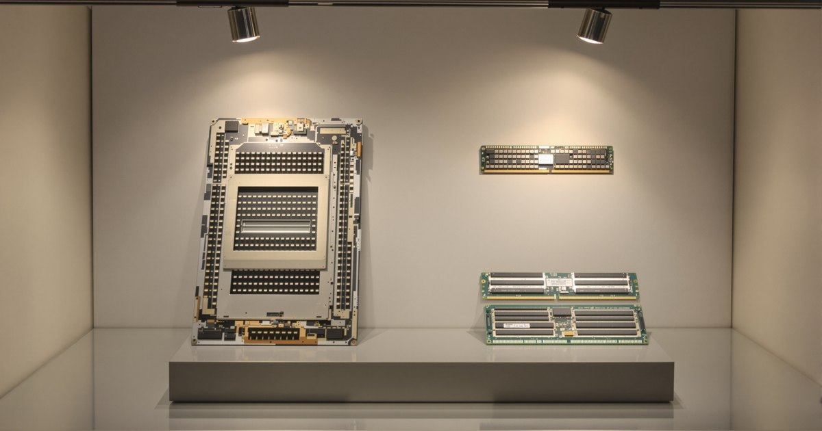
How RAM evolved alongside mainframes, minicomputers, PCs, servers and AI systems, and what each era changed about the modules we install today.
Every memory module NEMIX ships carries decisions made decades ago. The 8-bit byte, parity and ECC, the idea of a pluggable module, registered and load-reduced buffering, the width of a memory channel: each one was an answer to a problem some earlier machine ran into. This guide walks through eight eras of computing and follows one thread through all of them, the memory. Processors, storage and the machines themselves appear as context, because memory never evolved on its own. It evolved because something else got faster, bigger or cheaper and the memory had to keep up.
1. The mainframe era (1950s to 1960s): memory before the chip
The first electronic computers had almost nothing we would call RAM. ENIAC, completed in 1945, held its working numbers in vacuum-tube counters and was programmed by rewiring. The idea of a stored program, a machine that keeps its instructions in the same memory as its data, needed a memory that could be read and written at electronic speed, and the first attempts were strange. The Williams-Kilburn tube stored bits as charged spots on the face of a cathode-ray tube; the Manchester Baby ran the first stored program on one in June 1948. Mercury delay lines, used in EDSAC (1949) and UNIVAC I (1951), circulated bits as sound pulses through a tube of mercury and read them as they came out the other end. Both worked. Neither was reliable, and neither held more than a few thousand bits.
The answer came from MIT's Whirlwind project. Magnetic core memory, developed under Jay Forrester and running in Whirlwind by 1953, stored each bit as the magnetic direction of a tiny ferrite ring threaded on a grid of wires. It was random access in the full sense: any bit could be read in the same time as any other, it did not forget when the power went off, and it could be made in large arrays by hand. IBM put core in the 704 in 1954, and for the next two decades every serious computer used it. Core memory was also the first memory with a price per bit that people argued about, because the rings were strung by hand and the cost of the memory could exceed the cost of the processor.
The transistor (Bell Labs, 1947) replaced the vacuum tube in logic by the late 1950s, and the integrated circuit (Kilby in 1958, Noyce in 1959) put many transistors on one piece of silicon. Memory stayed magnetic longer than logic did. The era's defining machine, IBM's System/360 announced in April 1964, used core memory, and it fixed two conventions that are still in every module today: the 8-bit byte as the unit of addressing, and the practice of storing a check bit alongside the data so that a flipped bit could be detected. That check bit is the ancestor of the parity and ECC that server memory still uses.
What the era left behind: random access, the byte, and the first error checking. Memory as a separate component with its own cost curve.
2. The minicomputer revolution (1960s to 1970s): memory moves to silicon
Digital Equipment Corporation built computers that a laboratory or a department could afford. The PDP-8 of 1965 cost around $18,000 and sold in the tens of thousands; the PDP-11 of 1970 became the machine that Unix and C were written on, and the VAX-11/780 of 1977 brought 32-bit addressing and virtual memory to a box that fit in a room rather than a floor. Minicomputers mattered for memory because they made the market large. Thousands of machines needed memory, not dozens, and that volume justified building it on silicon.
The single-transistor DRAM cell was invented at IBM by Robert Dennard in 1966 and patented in 1968: one transistor and one capacitor per bit, with the charge on the capacitor standing for the data and a refresh cycle to top it up before it leaked away. Intel, founded in 1968 as a memory company, shipped the 1103 in October 1970. It held 1,024 bits. Within a few years it was the best-selling semiconductor in the world, and core memory, which had dominated for two decades, was obsolete by the middle of the 1970s. DRAM was smaller, cheaper to make, and got cheaper every year as the process shrank. The refresh requirement, the thing that puts the D in DRAM, is still the defining trait of main memory today.
The same company made a second decision in this era that shaped everything after it. In November 1971 Intel shipped the 4004, a processor on a single chip. The microprocessor and the DRAM chip arrived within a year of each other, and the two have been sized against each other ever since.
What the era left behind: DRAM. Memory as a volume semiconductor product rather than a hand-built assembly.
3. The personal computer (1970s to 1980s): memory on the motherboard
The Altair 8800 of January 1975 shipped with 256 bytes of memory and a row of switches. The Apple II (1977) came with 4KB and could take 48KB. The IBM PC of August 1981 had 16KB on the board, expandable to 256KB, on an Intel 8088. The first Macintosh (1984) had 128KB. These numbers look absurd now, but each was a serious engineering compromise between what the processor could address and what a buyer would pay.
Memory in this era was soldered or socketed directly on the motherboard as individual DRAM chips in DIP packages, the rectangular black chips with two rows of pins. Adding memory meant pressing in more chips, often in sets of nine: eight for data and one for parity, because IBM carried the mainframe habit of error checking into the PC. The PC's architecture also created one of the most famous limits in computing. The 8088 could address 1MB, IBM reserved the top 384KB for video and ROM, and the 640KB that remained became a wall that software ran into for a decade.
Storage changed shape too. Cassette tape gave way to floppy disks, then to the first hard drives in PCs (the IBM PC/XT of 1983 had a 10MB drive). None of this was fast. The gap between what a processor could do in a clock cycle and how fast memory could answer was already opening, and the first caches, small amounts of faster SRAM next to the processor, appeared in high-end systems to hide it.
What the era left behind: memory as something a user adds to a machine, parity on the desktop, and the address-space limit as a reason to upgrade.
4. The desktop era (1990s): modules, SDRAM and ECC in servers
The 1990s turned memory into a module. Pressing individual chips into sockets did not scale, so chips were soldered onto a small card with an edge connector: the SIMM. Thirty-pin SIMMs carried 8 data bits (9 with parity) and appeared in the late 1980s; 72-pin SIMMs carried 32 bits and matched the 486 and early Pentium. Because a Pentium had a 64-bit memory bus, 72-pin SIMMs had to be installed in pairs. The DIMM, with contacts on both sides of the card and a 64-bit data path, arrived with the 168-pin SDRAM module and removed the pairing requirement. Every memory module sold since, from RDIMMs to SODIMMs, descends from that design.
The DRAM inside the modules changed as well. Fast Page Mode and then EDO DRAM were asynchronous: the processor asked, waited, and got an answer. Synchronous DRAM, standardized by JEDEC in 1993 and mainstream by 1996 to 1998 as PC66, PC100 and PC133, ran on the same clock as the system bus and could pipeline requests. That one change, memory that answers in step with a clock, is the foundation of every DDR generation.
Error correction found its home in this decade. Parity could detect a flipped bit but not fix it. ECC, using a Hamming-style code across a 72-bit word (64 data bits plus 8 check bits), could correct a single-bit error and detect a double-bit error without stopping the machine. As Windows NT, Novell and the early web pushed PC-architecture servers into roles that mainframes and minis had held, ECC became the line between a desktop and a server. The Pentium Pro (1995) and its chipsets supported it, and server boards have expected it ever since. If you have ever wondered why server modules have nine chips per side instead of eight, this is the decade that decided it. Our ECC vs non-ECC guide covers what that extra chip does today.
Capacity went from megabytes to tens of megabytes on desktops. Windows 95 (1995) ran on 8MB and wanted 16MB. A 1999 workstation might carry 256MB. The memory types we sell today, unbuffered, registered, load-reduced and small-outline, all trace to form factors defined in this decade.
What the era left behind: the DIMM, synchronous memory, and ECC as the server standard.
5. The internet and mobile era (2000s): DDR and the laptop
SDRAM moved data once per clock cycle. Double Data Rate SDRAM moved data on both the rising and falling edge of the clock, doubling bandwidth at the same clock speed. JEDEC published the DDR standard in 2000, and the 184-pin DDR DIMM (PC1600 and PC2100, later PC3200) became the desktop and server standard within two years. DDR2 followed in 2003 on a 240-pin module, with lower voltage (1.8V from 2.5V) and a prefetch of four bits per clock instead of two, which let the internal DRAM run slower than the interface. DDR3 arrived in 2007, also 240-pin but keyed differently, at 1.5V with an 8-bit prefetch. The pattern was set: each generation roughly doubled bandwidth, cut voltage, and used a new key so the wrong module could not be inserted.
Servers needed more modules per channel than a processor could drive directly, so the registered DIMM, which puts a register chip on the module to buffer the address and command lines, became standard in the server tier during the DDR and DDR2 years. Registered modules add a clock of latency and cost a little more, in exchange for letting a board hold more memory. That trade-off is unchanged in the DDR5 RDIMMs in our catalog. A short-lived alternative, the Fully Buffered DIMM of 2006, put a serial interface on the module and was abandoned after one generation because of heat and latency. Industry memory of that experiment is part of why later buffering designs stayed parallel.
Mobile computing was the other force. Laptops needed a module half the length of a DIMM, and the small-outline DIMM, the SODIMM, became the laptop standard through DDR, DDR2 and DDR3. The iPhone (2007) and the smartphones that followed used soldered low-power DRAM instead, which is why phone memory has never been an upgrade. Storage began its own transition: NAND flash SSDs went from exotic to mainstream around 2008, and the gap between memory speed and storage speed, which had been three or four orders of magnitude for decades, started to close.
Multi-core processors arrived in this decade too (Intel's Core 2 Duo in 2006, AMD's Opteron dual-core in 2005), and two cores sharing one memory bus made memory bandwidth, not just capacity, a thing buyers had to think about. A workstation might carry 4GB to 8GB by 2009; a two-socket server 32GB to 64GB.
What the era left behind: the DDR cadence, registered modules as the server norm, and the SODIMM.
6. Multi-core, cloud and virtualization (2010 to 2020): DDR4 and the capacity race
Virtualization and the cloud changed what a server was for. A machine running VMware or a hypervisor at Amazon Web Services (launched 2006) was not running one workload but dozens, and every virtual machine wanted its own slice of RAM. Memory capacity per socket became the number that mattered, and the industry spent the decade pushing it up.
DDR4 was specified by JEDEC in 2012 and shipped in volume in 2014, with Intel's Haswell-E on the desktop and the Xeon E5 v3 in servers. It moved to a 288-pin module, 1.2V, and bank groups that let the DRAM keep more requests in flight. Speeds ran from DDR4-2133 at launch to DDR4-3200 as the mainstream server speed by 2019. Module capacity climbed through 16GB, 32GB and 64GB to 128GB and 256GB, using stacked dies (3DS) at the top end.
The load-reduced DIMM, introduced with DDR3 and widespread with DDR4, went a step beyond the registered DIMM: it buffers the data lines as well as the address lines, so a channel sees one electrical load per module however many DRAM chips are on it. LRDIMMs are what let a two-socket server reach 1TB, 2TB and beyond. They cost more and add latency, so most servers use RDIMMs and reach for LRDIMMs only at the highest capacities. The decision between the two is one we help customers with every day; the DDR4 RDIMM and LRDIMM collections cover the generation that most of the installed server base still runs.
AMD's return to servers with EPYC in 2017 brought eight memory channels per socket, up from four on most Intel parts, and made channel count a headline specification. Storage finished its transition: NVMe (specification 2011, drives from 2013) put flash on the PCIe bus and made the SSD the default. By 2020 a mainstream two-socket server carried 256GB to 1TB, and the memory in it often cost more than the processors.
What the era left behind: DDR4, LRDIMMs, channel count as a specification, and memory as the largest line item in a server.
7. High-performance and AI computing (2020 to today): DDR5, HBM and the memory wall
DDR5 was published by JEDEC in July 2020. Consumer platforms adopted it with Intel's Alder Lake in late 2021; servers followed with AMD's EPYC Genoa (November 2022, twelve channels per socket) and Intel's Sapphire Rapids (January 2023, eight channels). It is the largest architectural change to the module since the DIMM itself. Each DDR5 module is split into two independent 32-bit sub-channels (40 bits with ECC), which doubles the number of requests a channel can juggle. Voltage regulation moved from the motherboard onto the module as a power management IC, so the module controls its own supply. Every DDR5 DRAM chip has on-die ECC that corrects single-bit errors inside the chip, separate from the system-level ECC that a server RDIMM still provides. Launch speed was DDR5-4800; servers now run DDR5-5600 and DDR5-6400, with faster to come.
Capacity kept climbing with the DRAM die. 24Gb dies made 48GB and 96GB modules practical, and 128GB and 256GB RDIMMs now sit at the top of the range. A single socket with twelve channels and 256GB modules reaches 3TB of memory. Our DDR5 RDIMM collection runs from 16GB to 256GB across DDR5-4800, 5600 and 6400.
The AI boom changed the memory conversation again. Training and running large models is bound by memory bandwidth, not arithmetic, and the DRAM that feeds a GPU is High Bandwidth Memory: stacks of DRAM dies on the same package as the processor, connected through thousands of wires. HBM was standardized in 2013 and first shipped on AMD's Fiji GPUs in 2015. HBM2 (2016), HBM3 (2022, on NVIDIA's H100) and HBM3E (2024) each roughly doubled bandwidth, and HBM supply is now one of the constraints on how many AI accelerators the industry can build. HBM is soldered and unupgradeable, so it does not replace DIMMs. What it does is move the bottleneck: an AI server's system RAM has to stage data, hold model checkpoints and feed the GPUs, and AI servers need more system RAM, not less, as the accelerators get faster.
Workstations have had their own version of this. AMD's Threadripper PRO and Intel's Xeon W platforms bring eight-channel DDR5 RDIMM to a tower under a desk, and a single AI workstation can now carry more memory than a 2015 server rack.
What the era left behind: DDR5's sub-channels and on-module power, HBM as the GPU's memory, and bandwidth as the limiting resource.
8. What comes next: MRDIMM, CXL and beyond
Three developments are already in motion, and all three are answers to the same problem: processors have more cores than their memory channels can feed.
MRDIMM (multiplexed rank DIMM) puts a data buffer on the module that combines two ranks of DDR5 into one data stream running at twice the speed. JEDEC published the standard in 2024, and Intel's Xeon 6 platform (Granite Rapids, September 2024) was the first to support it, at DDR5-8800. It keeps the DIMM slot and the DDR5 DRAM while nearly doubling bandwidth per channel. Our guide to RDIMM vs MRDIMM vs MCRDIMM explains how the variants differ and which platforms take them.
CXL (Compute Express Link) is a protocol that runs over PCIe and lets a server attach memory outside the DIMM slots: on an add-in card, in a separate chassis, or shared between several processors. CXL 1.0 was published in March 2019, 2.0 in November 2020 and 3.0 in 2022. The first CXL memory expanders shipped with the Genoa and Sapphire Rapids generation. CXL memory is slower than a local DIMM, so the model is tiered: DDR5 in the slots for the hot data, CXL behind it for capacity. For buyers, it means a server's memory ceiling will no longer be fixed by its slot count.
DDR6 and HBM4 are the next steps on the two existing lines. JEDEC published the HBM4 standard in 2025, with wider interfaces and higher stacks for the next accelerator generation. DDR6 is in definition, targeting roughly double DDR5's launch bandwidth, with first platforms expected late in the decade. Further out, memory built on new physics (MRAM, phase-change and others) has been promised for twenty years and has found niches, but DRAM's cost per bit has kept it as main memory, and nothing on the current roadmap displaces it before 2030.
Quantum computers, often mentioned in the same breath, use a different kind of state entirely and still rely on conventional computers, with conventional memory, to control them. They extend the story rather than ending it.
Timeline: landmark systems and the memory inside them
| Year | System or technology | Memory |
|---|---|---|
| 1945 | ENIAC | Vacuum-tube counters, about 20 ten-digit numbers |
| 1948 | Manchester Baby | Williams-Kilburn tube, 1,024 bits; first stored program |
| 1951 | UNIVAC I | Mercury delay lines, 1,000 words |
| 1953 | MIT Whirlwind | First magnetic core memory in a working computer |
| 1964 | IBM System/360 | Core memory; 8-bit byte and memory checking standardized |
| 1965 | DEC PDP-8 | 4K words of core; the first mass-market minicomputer |
| 1970 | Intel 1103 | First commercial DRAM, 1Kb |
| 1971 | Intel 4004 | First microprocessor |
| 1977 | Apple II; DEC VAX-11/780 | 4KB to 48KB DRAM; 32-bit virtual memory |
| 1981 | IBM PC | 16KB to 256KB DRAM chips on the board, with parity |
| Late 1980s | 30-pin SIMM | First pluggable memory module |
| 1993 | Intel Pentium; JEDEC SDRAM; NEMIX founded | 64-bit memory bus; synchronous DRAM standardized |
| 1995 | Pentium Pro, Windows 95 | ECC in PC-architecture servers; 168-pin DIMM |
| 2000 | DDR SDRAM | 184-pin DIMM, 2.5V |
| 2003 | DDR2 | 240-pin DIMM, 1.8V |
| 2006 | Intel Core 2 Duo; Amazon Web Services | Multi-core and cloud raise capacity demand |
| 2007 | DDR3; iPhone | 240-pin DIMM, 1.5V; soldered LPDDR in phones |
| 2012 | DDR3 LRDIMM (Xeon E5) | Load reduction for high-capacity servers |
| 2014 | DDR4 | 288-pin DIMM, 1.2V |
| 2015 | AMD Fiji GPU | First HBM |
| 2017 | AMD EPYC | Eight memory channels per socket |
| 2019 | CXL 1.0 | Memory attached over PCIe |
| 2020 | DDR5 standard | Two sub-channels per module, on-module PMIC, on-die ECC |
| 2022 | NVIDIA H100; AMD EPYC Genoa | HBM3; twelve DDR5 channels per socket |
| 2024 | MRDIMM; HBM3E | DDR5-8800 on Xeon 6; next HBM generation |
| 2025 | HBM4 standard | Wider interface for next-generation accelerators |
Frequently asked questions
When was DRAM invented?
The single-transistor DRAM cell was invented at IBM by Robert Dennard in 1966 and patented in 1968. The first commercial DRAM chip was the Intel 1103, a 1Kb part shipped in October 1970. Core memory was obsolete within about five years.
What is the difference between DDR4 and DDR5 memory?
DDR5 splits each module into two independent 32-bit sub-channels, moves voltage regulation onto the module as a PMIC, adds on-die ECC inside every DRAM chip, and starts at DDR5-4800 against DDR4's DDR4-2133. The modules are keyed differently and are not interchangeable.
What is HBM and does it replace DIMMs?
High Bandwidth Memory is DRAM stacked on the same package as a GPU or accelerator. It gives far more bandwidth than DIMMs but is soldered and cannot be upgraded, so it feeds the accelerator while system RAM in DIMM slots stages data, holds checkpoints and runs the host.
What is an MRDIMM?
A multiplexed rank DIMM puts a data buffer on a DDR5 module that combines two ranks into one data stream at twice the speed, reaching DDR5-8800 on supported platforms. JEDEC published the standard in 2024 and Intel Xeon 6 was the first platform to support it.
What this history means when you buy memory
Almost every rule a memory buyer follows has a date attached to it. Install modules in matched sets because the Pentium's 64-bit bus needed pairs of 32-bit SIMMs, and today's multi-channel controllers still want every channel filled evenly. Use ECC in a server because 1990s servers inherited the mainframe's check bit and the operating systems that run on them expect it. Choose registered over unbuffered when a board carries many modules because the DDR-era register solved an electrical problem that has not gone away. Choose load-reduced only at the top of the capacity range because the buffer costs latency. Check the platform's supported speed because DDR5's speed grades, like every generation before, outrun what a given processor will actually clock.
NEMIX has been selecting and compatibility-testing memory since 1993, which is to say since the SIMM and the first SDRAM. The memory types guide explains the current families in detail, and the DDR5 memory and DDR4 RDIMM collections cover the two generations in production today. If your system is on the timeline above, there is a good chance we have the module for it.